Math Is Fun Forum
You are not logged in.
- Topics: Active | Unanswered
Pages: 1
#1 Today 18:28:38
- Jai Ganesh
- Administrator

- Registered: 2005-06-28
- Posts: 53,104
Transistor
Transistor
Gist
A transistor is a semiconductor device that amplifies or switches electronic signals and power, acting as a fundamental building block of modern electronics, found in everything from smartphones to computers. It uses a small current or voltage at one terminal to control a much larger current flow between the other two, functioning like a tiny, fast electronic switch or amplifier.
A transistor is a semiconductor device that acts as either an electronic switch (turning current on/off) or an amplifier (boosting signals), controlling a larger current with a smaller one, forming the fundamental building block of modern electronics like computers, radios, and smartphones.
Summary
A transistor is a semiconductor device used to amplify or switch electrical signals and power. It is one of the basic building blocks of modern electronics. It is composed of semiconductor material, usually with at least three terminals for connection to an electronic circuit. A voltage or current applied to one pair of the transistor's terminals controls the current through another pair of terminals. Because the controlled (output) power can be higher than the controlling (input) power, a transistor can amplify a signal. Some transistors are packaged individually, but many more in miniature form are found embedded in integrated circuits. Because transistors are the key active components in practically all modern electronics, many people consider them one of the 20th century's greatest inventions.
Physicist Julius Edgar Lilienfeld proposed the concept of a field-effect transistor (FET) in 1925, but it was not possible to construct a working device at that time. The first working device was a point-contact transistor invented in 1947 by physicists John Bardeen, Walter Brattain, and William Shockley at Bell Labs who shared the 1956 Nobel Prize in Physics for their achievement. The most widely used type of transistor, the metal–oxide–semiconductor field-effect transistor (MOSFET), was invented at Bell Labs between 1955 and 1960. Transistors revolutionized the field of electronics and paved the way for smaller and cheaper radios, calculators, computers, and other electronic devices.
Most transistors are made from very pure silicon, and some from germanium, but certain other semiconductor materials are sometimes used. A transistor may have only one kind of charge carrier in a field-effect transistor, or may have two kinds of charge carriers in bipolar junction transistor devices. Compared with the vacuum tube, transistors are generally smaller and require less power to operate. Certain vacuum tubes have advantages over transistors at very high operating frequencies or high operating voltages, such as traveling-wave tubes and gyrotrons. Many types of transistors are made to standardized specifications by multiple manufacturers.
Details
A transistor is a semiconductor device for amplifying, controlling, and generating electrical signals. Transistors are the active components of integrated circuits, or “microchips,” which often contain billions of these minuscule devices etched into their shiny surfaces. Deeply embedded in almost everything electronic, transistors have become the nerve cells of the Information Age.
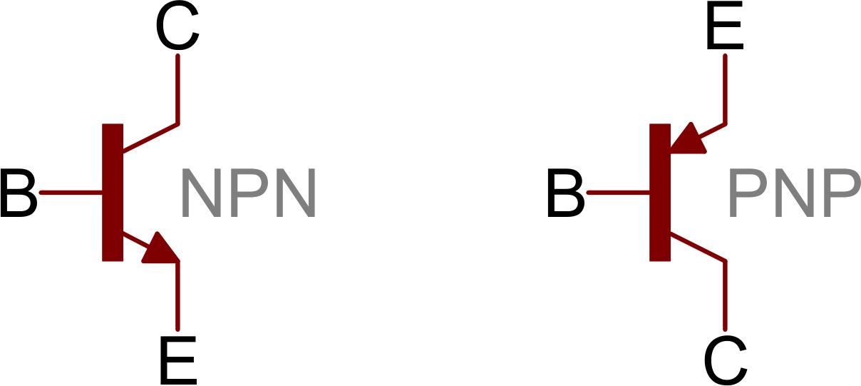
There are typically three electrical leads in a transistor, called the emitter, the collector, and the base—or, in modern switching applications, the source, the drain, and the gate. An electrical signal applied to the base (or gate) influences the semiconductor material’s ability to conduct electrical current, which flows between the emitter (or source) and collector (or drain) in most applications. A voltage source such as a battery drives the current, while the rate of current flow through the transistor at any given moment is governed by an input signal at the gate—much as a faucet valve is used to regulate the flow of water through a garden hose.
The first commercial applications for transistors were for hearing aids and “pocket” radios during the 1950s. With their small size and low power consumption, transistors were desirable substitutes for the vacuum tubes (known as “valves” in Great Britain) then used to amplify weak electrical signals and produce audible sounds. Transistors also began to replace vacuum tubes in the oscillator circuits used to generate radio signals, especially after specialized structures were developed to handle the higher frequencies and power levels involved. Low-frequency, high-power applications, such as power-supply inverters that convert alternating current (AC) into direct current (DC), have also been transistorized. Some power transistors can now handle currents of hundreds of amperes at electric potentials over a thousand volts.
By far the most common application of transistors today is for computer memory chips—including solid-state multimedia storage devices for electronic games, cameras, and MP3 players—and microprocessors, where millions of components are embedded in a single integrated circuit. Here the voltage applied to the gate electrode, generally a few volts or less, determines whether current can flow from the transistor’s source to its drain. In this case the transistor operates as a switch: if a current flows, the circuit involved is on, and if not, it is off. These two distinct states, the only possibilities in such a circuit, correspond respectively to the binary 1s and 0s employed in digital computers. Similar applications of transistors occur in the complex switching circuits used throughout modern telecommunications systems. The potential switching speeds of these transistors now are hundreds of gigahertz, or more than 100 billion on-and-off cycles per second.
Development of transistors
The transistor was invented in 1947–48 by three American physicists, John Bardeen, Walter H. Brattain, and William B. Shockley, at the American Telephone and Telegraph Company’s Bell Laboratories. The transistor proved to be a viable alternative to the electron tube and, by the late 1950s, supplanted the latter in many applications. Its small size, low heat generation, high reliability, and low power consumption made possible a breakthrough in the miniaturization of complex circuitry. During the 1960s and ’70s, transistors were incorporated into integrated circuits, in which a multitude of components (e.g., diodes, resistors, and capacitors) are formed on a single “chip” of semiconductor material.
Motivation and early radar research
Electron tubes are bulky and fragile, and they consume large amounts of power to heat their cathode filaments and generate streams of electrons; also, they often burn out after several thousand hours of operation. Electromechanical switches, or relays, are slow and can become stuck in the on or off position. For applications requiring thousands of tubes or switches, such as the nationwide telephone systems developing around the world in the 1940s and the first electronic digital computers, this meant constant vigilance was needed to minimize the inevitable breakdowns.
An alternative was found in semiconductors, materials such as silicon or germanium whose electrical conductivity lies midway between that of insulators such as glass and conductors such as aluminum. The conductive properties of semiconductors can be controlled by “doping” them with select impurities, and a few visionaries had seen the potential of such devices for telecommunications and computers. However, it was military funding for radar development in the 1940s that opened the door to their realization. The “superheterodyne” electronic circuits used to detect radar waves required a diode rectifier—a device that allows current to flow in just one direction—that could operate successfully at ultrahigh frequencies over one gigahertz. Electron tubes just did not suffice, and solid-state diodes based on existing copper-oxide semiconductors were also much too slow for this purpose.
Crystal rectifiers based on silicon and germanium came to the rescue. In these devices a tungsten wire was jabbed into the surface of the semiconductor material, which was doped with tiny amounts of impurities, such as boron or phosphorus. The impurity atoms assumed positions in the material’s crystal lattice, displacing silicon (or germanium) atoms and thereby generating tiny populations of charge carriers (such as electrons) capable of conducting usable electrical current. Depending on the nature of the charge carriers and the applied voltage, a current could flow from the wire into the surface or vice-versa, but not in both directions. Thus, these devices served as the much-needed rectifiers operating at the gigahertz frequencies required for detecting rebounding microwave radiation in military radar systems. By the end of World War II, millions of crystal rectifiers were being produced annually by such American manufacturers as Sylvania and Western Electric.
Innovation at Bell Labs
Executives at Bell Labs had recognized that semiconductors might lead to solid-state alternatives to the electron-tube amplifiers and electromechanical switches employed throughout the nationwide Bell telephone system. In 1936 the new director of research at Bell Labs, Mervin Kelly, began recruiting solid-state physicists. Among his first recruits was William B. Shockley, who proposed a few amplifier designs based on copper-oxide semiconductor materials then used to make diodes. With the help of Walter H. Brattain, an experimental physicist already working at Bell Labs, he even tried to fabricate a prototype device in 1939, but it failed completely. Semiconductor theory could not yet explain exactly what was happening to electrons inside these devices, especially at the interface between copper and its oxide. Compounding the difficulty of any theoretical understanding was the problem of controlling the exact composition of these early semiconductor materials, which were binary combinations of different chemical elements (such as copper and oxygen).
With the close of World War II, Kelly reorganized Bell Labs and created a new solid-state research group headed by Shockley. The postwar search for a solid-state amplifier began in April 1945 with Shockley’s suggestion that silicon and germanium semiconductors could be used to make a field-effect amplifier (see integrated circuit: Field-effect transistors). He reasoned that an electric field from a third electrode could increase the conductivity of a sliver of semiconductor material just beneath it and thereby allow usable current to flow through the sliver. But attempts to fabricate such a device by Brattain and others in Shockley’s group again failed. The following March, John Bardeen, a theoretical physicist whom Shockley had hired for his group, offered a possible explanation. Perhaps electrons drawn to the semiconductor surface by the electric field were blocking the penetration of this field into the bulk material, thereby preventing it from influencing the conductivity.
Bardeen’s conjecture spurred a basic research program at Bell Labs into the behaviour of these “surface-state” electrons. While studying this phenomenon in November 1947, Brattain stumbled upon a way to neutralize their blocking effect and permit the applied field to penetrate deep into the semiconductor material. Working closely together over the next month, Bardeen and Brattain invented the first successful semiconductor amplifier, called the point-contact transistor, on December 16, 1947. Similar to the World War II crystal rectifiers, this weird-looking device had not one but two closely spaced metal wires jabbing into the surface of a semiconductor—in this case, germanium. The input signal on one of these wires (the emitter) boosted the conductivity of the germanium beneath both of them, thus modulating the output signal on the other wire (the collector). Observers present at a demonstration of this device the following week could hear amplified voices in the earphones that it powered. Shockley later called this invention a “magnificent Christmas present” for the farsighted company, which had supported the research program that made this breakthrough.
Not to be outdone by members of his own group, Shockley conceived yet another way to fabricate a semiconductor amplifier the very next month, on January 23, 1948. His junction transistor was basically a three-layer sandwich of germanium or silicon in which the adjacent layers would be doped with different impurities to induce distinct electrical characteristics. An input signal entering the middle layer—the “meat” of the semiconductor sandwich—determined how much current flowed from one end of the device to the other under the influence of an applied voltage. Shockley’s device is often called the bipolar junction transistor because its operation requires that the negatively charged electrons and their positively charged counterparts (the holes corresponding to an absence of electrons in the crystal lattice) coexist briefly in the presence of one another.
The name transistor, a combination of transfer and resistor, was coined for these devices in May 1948 by Bell Labs electrical engineer John Robinson Pierce, who was also a science-fiction author in his spare time. A month later Bell Labs announced the revolutionary invention in a press conference held at its New York City headquarters, heralding Bardeen, Brattain, and Shockley as the three coinventors of the transistor. The three were eventually awarded the Nobel Prize for Physics for their invention.
Although the point-contact transistor was the first transistor invented, it faced a difficult gestation period and was eventually used only in a switch made for the Bell telephone system. Manufacturing them reliably and with uniform operating characteristics proved a daunting problem, largely because of hard-to-control variations in the metal-to-semiconductor point contacts.
Shockley had foreseen these difficulties in the process of conceiving the junction transistor, which he figured would be much easier to manufacture. But it still required more than three years, until mid-1951, to resolve its own development problems. Bell Labs scientists, engineers, and technicians first had to find ways to make ultrapure germanium and silicon, form large crystals of these elements, dope them with narrow layers of the required impurities, and attach delicate wires to these layers to serve as electrodes. In July 1951 Bell Labs announced the successful invention and development of the junction transistor, this time with only Shockley in the spotlight.
Commercialization
Commercial transistors began to roll off production lines during the 1950s, after Bell Labs licensed the technology of their production to other companies, including General Electric, Raytheon, RCA, Sylvania, and Transitron Electronics. Transistors found ready applications in lightweight devices such as hearing aids and portable radios. Texas Instruments Inc., working with the Regency Division of Industrial Development Engineering Associates, manufactured the first transistor radio in late 1954. Selling for $49.95, the Regency TR-1 employed four germanium junction transistors in a multistage amplifier of radio signals. The very next year a new Japanese company, Sony, introduced its own transistor radio and began to corner the market for this and other transistorized consumer electronics.
Transistors also began replacing vacuum tubes in the digital computers manufactured by IBM, Control Data, and other companies. “It seems to me that in these robot brains the transistor is the ideal nerve cell,” Shockley had observed in a 1949 radio interview. “The advantage of the transistor is that it is inherently a small-size and low-power device,” noted Bell Labs circuit engineer Robert Wallace early in the 1950s. “This means you can pack a large number of them in a small space without excessive heat generation and achieve low propagation delays. And that’s what you need for logic applications. The significance of the transistor is not that it can replace the tube but that it can do things the vacuum tube could never do!” After 1955 IBM started purchasing germanium transistors from Texas Instruments to employ in its computer circuits. By the end of the 1950s, bipolar junction transistors had almost completely replaced electron tubes in computer applications.
Silicon transistors
During the 1950s, meanwhile, scientists and engineers at Bell Labs and Texas Instruments were developing advanced technologies needed to produce silicon transistors. Because of its higher melting temperature and greater reactivity, silicon was much more difficult to work with than germanium, but it offered major prospects for better performance, especially in switching applications. Germanium transistors make leaky switches; substantial leakage currents can flow when these devices are supposedly in their off state. Silicon transistors have far less leakage. In 1954 Texas Instruments produced the first commercially available silicon junction transistors and quickly dominated this new market—especially for military applications, in which their high cost was of little concern.
In the mid-1950s Bell Labs focused its transistor-development efforts around new diffusion technologies, in which very narrow semiconductor layers—with thicknesses measured in microns, or millionths of a metre—are prepared by diffusing impurity atoms into the semiconductor surface from a hot gas. Inside a diffusion furnace the impurity atoms penetrate more readily into the silicon or germanium surface; their penetration depth is controlled by varying the density, temperature, and pressure of the gas as well as the processing time. (See integrated circuit: Fabricating ICs.) For the first time, diodes and transistors produced by these diffusion implantation processes functioned at frequencies above 100 megahertz (100 million cycles per second). These diffused-base transistors could be used in receivers and transmitters for FM radio and television, which operate at such high frequencies.
Another important breakthrough occurred at Bell Labs in 1955, when Carl Frosch and Link Derick developed a means of producing a glassy silicon dioxide outer layer on the silicon surface during the diffusion process. This layer offered transistor producers a promising way to protect the silicon underneath from further impurities once the diffusion process was finished and the desired electrical properties had been established.
Texas Instruments, Fairchild Semiconductor Corporation, and other companies took the lead in applying these diffusion technologies to the large-scale manufacture of transistors. At Fairchild, physicist Jean Hoerni developed the planar manufacturing process, whereby the various semiconductor layers and their sensitive interfaces are embedded beneath a protective silicon dioxide outer layer. The company was soon making and selling planar silicon transistors, largely for military applications. Led by Robert Noyce and Gordon E. Moore, Fairchild’s scientists and engineers extended this revolutionary technique to the manufacture of integrated circuits.
In the late 1950s Bell Labs researchers developed ways to use the new diffusion technologies to realize Shockley’s original 1945 idea of a field-effect transistor (FET). To do so, they had to overcome the problem of surface-state electrons, which would otherwise have blocked external electric fields from penetrating into the semiconductor. They succeeded by carefully cleaning the silicon surface and growing a very pure silicon dioxide layer on it. This approach reduced the number of surface-state electrons at the interface between the silicon and oxide layers, permitting fabrication of the first successful field-effect transistor in 1960 at Bell Labs—which, however, did not pursue its development any further.
Refinements of the FET design by other companies, especially RCA and Fairchild, resulted in the metal-oxide-semiconductor field-effect transistor (MOSFET) during the early 1960s. The key problems to be solved were the stability and reliability of these MOS transistors, which relied upon interactions occurring at or near the sensitive silicon surface rather than deep inside. The two firms began to make MOS transistors commercially available in late 1964.
In early 1963 Frank Wanlass at Fairchild developed the complementary MOS (CMOS) transistor circuit, based on a pair of MOS transistors. This approach eventually proved ideal for use in integrated circuits because of its simplicity of production and very low power dissipation during standby operation. Stability problems continued to plague MOS transistors, however, until researchers at Fairchild developed solutions in the mid-1960s. By the end of the decade, MOS transistors were beginning to displace bipolar junction transistors in microchip manufacturing. Since the late 1980s CMOS has been the technology of choice for digital applications, while bipolar transistors are now used primarily for analog and microwave devices.
Transistor principles
The operation of junction transistors, as well as most other semiconductor devices, depends heavily on the behaviour of electrons and holes at the interface between two dissimilar layers, known as a p-n junction. Discovered in 1940 by Bell Labs electrochemist Russell Ohl, p-n junctions are formed by adding two different impurity elements to adjacent regions of germanium or silicon. The addition of these impurity elements is called doping. Atoms of elements from Group 15 of the periodic table (which possess five valence electrons), such as phosphorus or math, contribute an electron that has no natural resting place within the crystal lattice. These excess electrons are therefore loosely bound and relatively free to roam about, acting as charge carriers that can conduct electrical current. Atoms of elements from Group 13 (which have three valence electrons), such as boron or aluminum, induce a deficit of electrons when added as impurities, effectively creating “holes” in the lattice. These positively charged quantum mechanical entities are also fairly free to roam around and conduct electricity. Under the influence of an electric field, the electrons and holes move in opposite directions. During and immediately after World War II, chemists and metallurgists at Bell Labs perfected techniques of adding impurities to high-purity silicon and germanium to induce the desired electron-rich layer (known as the n-layer) and the electron-poor layer (known as the p-layer) in these semiconductors, as described in the section Development of transistors.
A p-n junction acts as a rectifier, similar to the old point-contact crystal rectifiers, permitting easy flow of current in only a single direction. If no voltage is applied across the junction, electrons and holes will gather on opposite sides of the interface to form a depletion layer that will act as an insulator between the two sides. A negative voltage applied to the n-layer will drive the excess electrons within it toward the interface, where they will combine with the positively charged holes attracted there by the electric field. Current will then flow easily. If instead a positive voltage is applied to the n-layer, the resulting electric field will draw electrons away from the interface, so combinations of them with holes will occur much less often. In this case current will not flow (other than tiny leakage currents). Thus, electricity will flow in only one direction through a p-n junction.
Junction transistors
Shortly after his colleagues John Bardeen and Walter H. Brattain invented their point-contact device, Bell Labs physicist William B. Shockley recognized that these rectifying characteristics might also be used in making a junction transistor. In a 1949 paper Shockley explained the physical principles behind the operation of these junctions and showed how to use them in a three-layer—n-p-n or p-n-p—device that could act as a solid-state amplifier or switch. Electric current would flow from one end to the other, with the voltage applied to the inner layer governing how much current rushed by at any given moment. In the n-p-n junction transistor, for example, electrons would flow from one n-layer through the inner p-layer to the other n-layer. Thus, a weak electrical signal applied to the inner, base layer would modulate the current flowing through the entire device. For this current to flow, some of the electrons would have to survive briefly in the presence of holes; in order to reach the second n-layer, they could not all combine with holes in the p-layer. Such bipolar operation was not at all obvious when Shockley first conceived his junction transistor. Experiments with increasingly pure crystals of silicon and germanium showed that it indeed occurred, making bipolar junction transistors possible.
To achieve bipolar operation, it also helps that the base layer be narrow, so that electrons (in n-p-n transistors) and holes (in p-n-p) do not have to travel very far in the presence of their opposite numbers. Narrow base layers also promote high-frequency operation of junction transistors: the narrower the base, the higher the operating frequency. That is a major reason why there was so much interest in developing diffused-base transistors during the 1950s, as described in the section Silicon transistors. Their microns-thick bases permitted transistors to operate above 100 megahertz (100 million cycles per second) for the first time.
MOS-type transistors
A similar principle applies to metal-oxide-semiconductor (MOS) transistors, but here it is the distance between source and drain that largely determines the operating frequency. In an n-channel MOS (NMOS) transistor, for example, the source and the drain are two n-type regions that have been established in a piece of p-type semiconductor, usually silicon. Except for the two points at which metal leads contact these regions, the entire semiconductor surface is covered by an insulating oxide layer. The metal gate, usually aluminum, is deposited atop the oxide layer just above the gap between source and drain. If there is no voltage (or a negative voltage) upon the gate, the semiconductor material beneath it will contain excess holes, and very few electrons will be able to cross the gap, because one of the two p-n junctions will block their path. Therefore, no current will flow in this configuration—other than unavoidable leakage currents. If the gate voltage is instead positive, an electric field will penetrate through the oxide layer and attract electrons into the silicon layer (often called the inversion layer) directly beneath the gate. Once this voltage exceeds a specific threshold value, electrons will begin flowing easily between source and drain. The transistor turns on.
Analogous behaviour occurs in a p-channel MOS transistor, in which the source and the drain are p-type regions formed in n-type semiconductor material. Here a negative voltage above a threshold induces a layer of holes (instead of electrons) beneath the gate and permits a current of them to flow from source to drain. For both n-channel and p-channel MOS (also called NMOS and PMOS) transistors, the operating frequency is largely governed by the speed at which the electrons or holes can drift through the semiconductor material divided by the distance from source to drain. Because electrons have mobilities through silicon that are about three times higher than holes, NMOS transistors can operate at substantially higher frequencies than PMOS transistors. Small separations between source and drain also promote high-frequency operation, and extensive efforts have been devoted to reducing this distance.
In the 1960s Frank Wanlass of Fairchild Semiconductor recognized that combinations of an NMOS and a PMOS transistor would draw extremely little current in standby operation—just the tiny, unavoidable leakage currents. These CMOS, or complementary metal-oxide-semiconductor, transistor circuits consume significant power only when the gate voltage exceeds some threshold and a current flows from source to drain. Thus, they can serve as very low-power devices, often a million times lower than the equivalent bipolar junction transistors. Together with their inherent simplicity of fabrication, this feature of CMOS transistors has made them the natural choice for manufacturing microchips, which today cram millions of transistors into a surface area smaller than a fingernail. In such cases the waste heat generated by the component’s power consumption must be kept to an absolute minimum, or the chips will simply melt.
Field-effect transistors
Another kind of unipolar transistor, called the metal-semiconductor field-effect transistor (MESFET), is particularly well suited for microwave and other high-frequency applications because it can be manufactured from semiconductor materials with high electron mobilities that do not support an insulating oxide surface layer. These include compound semiconductors such as germanium-silicon and gallium math. A MESFET is built much like a MOS transistor but with no oxide layer between the gate and the underlying conduction channel. Instead, the gate makes a direct, rectifying contact with the channel, which is generally a thin layer of n-type semiconductor supported underneath by an insulating substrate. A negative voltage on the gate induces a depletion layer just beneath it that restricts the flow of electrons between source and drain. The device acts like a voltage-controlled resistor; if the gate voltage is large enough, it can block this flow almost completely. By contrast, a positive voltage on the gate encourages electrons to traverse the channel.
To improve MESFET performance even further, advanced devices known as heterojunction field-effect transistors have been developed, in which p-n junctions are established between two slightly dissimilar semiconductor materials, such as gallium math and aluminum gallium math. By properly controlling the impurities in the two substances, a high-conductivity channel can be formed at their interface, promoting the flow of electrons through it. If one semiconductor is a high-purity material, its electron mobility can be large, resulting in a high operating frequency for this kind of transistor. (The electron mobility of gallium math, for example, is five times that of silicon.) Heterojunction MESFETs are increasingly used for microwave applications such as cellular telephone systems.
Transistors and Moore’s law
In 1965, four years after Fairchild Semiconductor Corporation and Texas Instruments Inc. marketed their first integrated circuits, Fairchild research director Gordon E. Moore made a prediction in a special issue of Electronics magazine. Observing that the total number of components in these circuits had roughly doubled each year, he blithely extrapolated this annual doubling to the next decade, estimating that microcircuits of 1975 would contain an astounding 65,000 components per chip.
History proved Moore correct. His bold extrapolation has since become enshrined as Moore’s law—though its doubling period was lengthened to 18 months in the mid-1970s. What has made this dramatic explosion in circuit complexity possible is the steadily shrinking size of transistors over the decades. Measured in millimetres in the late 1940s, the dimensions of a typical transistor are typically about 10 nanometres, a reduction factor of over 100,000. Submicron transistor features were attained during the 1980s, when dynamic random-access memory (DRAM) chips began offering megabit storage capacities. At the dawn of the 21st century, these features approached 0.1 micron across, which allowed the manufacture of gigabit memory chips and microprocessors that operate at gigahertz frequencies. Moore’s law continued into the second decade of the 21st century with the introduction of three-dimensional transistors that were tens of nanometres in size.
As the size of transistors has shrunk, their cost has plummeted correspondingly from tens of dollars apiece to thousandths of a penny. As Moore was fond of saying, every year more transistors are produced than raindrops over California, and it costs less to make one than to print a single character on the page of a book. They are by far the most common human artifact on the planet. Deeply embedded in everything electronic, transistors permeate modern life almost as thoroughly as molecules permeate matter. Cheap, portable, and reliable equipment based on this remarkable device can be found in almost any village and hamlet in the world. This tiny invention, by making possible the Information Age, has transformed the world into a truly global society, making it a far more intimately connected place than ever before.
Additional Information:
What is a transistor?
Transistors are the key building blocks of integrated circuits and microchips. They’re basically microscopic electronic switches or amplifiers. As such, they control the flow of electrical signals, enabling the chip to process and store information.
A transistor is usually made from silicon or another semiconductor material. The properties of these types of material are in between those of an electric conductive material (like a metal) and an insulator (like rubber).
Depending on the temperature, for example, or on the presence of impurities, they can either conduct or block electricity. This makes them perfectly suited to control electrical signals.
A transistor consists of three terminals: the base, collector, and emitter. Through these terminals, the transistor can control the flow of current in a circuit.
How does a transistor work?
When a small electrical current is applied to the transistor base, it allows a larger current to flow between the collector and the emitter. This is like a valve: a little pressure on the base controls a much bigger flow of electricity.
* If there is no current at the base, the transistor acts like a closed switch. No current flows between the collector and emitter.
* If there is a current at the base, the transistor opens up. Current flows through.
This ability to control electrical current allows transistors to work as a switch (switching things on and off) or as an amplifier (making signals stronger).
* As a switch: Transistors can rapidly turn on and off, representing binary states (0 and 1) that form the foundation of digital computing. When a small voltage is applied to the base terminal, it allows a larger current to flow between the collector and emitter, switching the transistor ‘on.’ When the voltage is removed, the current stops, and the transistor turns ‘off.’
* As an amplifier: Transistors can also be used to boost weak electrical signals. A small input signal applied to the base can control a larger output signal between the collector and emitter, amplifying it. This is essential in devices like radios, televisions, and audio systems, where signal amplification is necessary for proper operation.
In digital electronics, transistors are used in large numbers to build logic gates. These form the foundation of computer processors. By switching on and off very quickly, transistors help process the binary code that computers use to operate.
The first transistors
The history of transistors starts in the 1940s. Scientists were looking for better ways to control electrical signals in devices like radios and televisions. At the time, these devices used vacuum tubes, which were big, used a lot of power, and often broke.
In 1947, three scientists at Bell Labs—John Bardeen, Walter Brattain, and William Shockley—created the first working transistor. This compact device could do the same job as a vacuum tube. But it was much smaller, used less power, and was more reliable.
By the 1950s, transistors were used in radios and early computers, making these devices smaller and easier to carry around. In 1956, MIT created the first computer that used transistors instead of vacuum tubes, showing just how useful they were for building faster, more efficient machines. By the 1960s, scientists figured out how to put many transistors onto a single chip. This lead to the creation of increasingly more powerful computer chips.
Why are transistors so important?
Transistors are the core components in integrated circuits and chips. Today’s microchips can contain billions of transistors, allowing devices to perform complex tasks at high speeds while using less power. Their invention and continuous miniaturizations revolutionized electronics. They make it possible to build smaller, faster, and more efficient devices.
Today, transistors are everywhere—in smartphones, laptops, and virtually all electronic devices. They are the key to the digital world we live in, and keep getting smaller and more powerful as technology improves.
It appears to me that if one wants to make progress in mathematics, one should study the masters and not the pupils. - Niels Henrik Abel.
Nothing is better than reading and gaining more and more knowledge - Stephen William Hawking.
Offline
Pages: 1